2D Single Crystal Metals for Nanophotonics
The study published in Nature Communications introduces a novel technique for fabricating large-area single-crystal 2D gold flakes with a nanometer scale thickness using a chemical etching method. These 2D gold flakes exhibit unique properties that enable the creation of plasmonic nanostructures with nanoscale optical confinement. This advancement holds promise for applications in the field of nanophotonics, enhancing light-matter interactions at the nanoscale.
Challenges in Previous Methods
While wet chemical methods have been previously utilized to prepare ultrathin 2D gold flakes, challenges arose due to difficulties in precisely controlling the thickness and size over time. These limitations hindered the optimization of optical and electrical properties crucial for various applications.
Preparation and Etching of 2D Gold Flakes
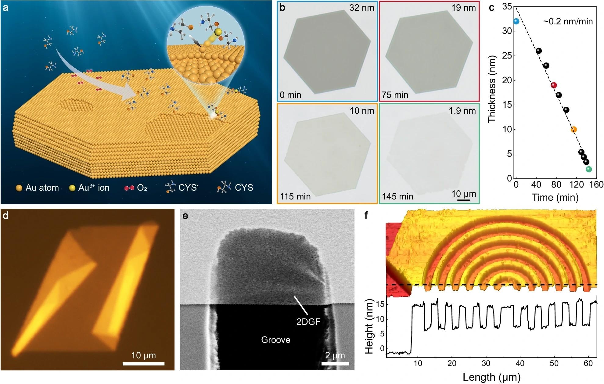
In this study, 2D gold flakes were prepared and transferred using a polydimethylsiloxane (PDMS)-assisted method, followed by patterning with electron beam lithography (EBL). The atomic-level precision etching (ALPE) approach involved etching with an aqueous solution of cysteamine to achieve controlled thickness reduction.
Insightful Results and Observations
Analyzing the atomic force microscopy (AFM) images of the etched gold flakes revealed a uniform monolayer-by-monolayer etching process that maintained the flakes’ initial quality, resulting in large-area gold flakes of uniform thickness. The single-crystal structure demonstrated excellent continuity and promising electrical properties.
Noteworthy Findings and Applications
The study highlights the effectiveness of the ALPE method in fabricating 2D gold flakes with exceptional optical properties, attributed to their quantum effects at reduced thickness. The etching rate and controllability of thickness were key factors in achieving high-quality gold flakes. Furthermore, the potential applications extend to transparent and flexible electrodes in optoelectronic devices, emphasizing the versatility of these 2D gold flakes.
Conclusive Insights
In conclusion, the research provides valuable insights into the fabrication of 2D single-crystal gold flakes with minimal thickness for nanophotonics applications. The innovative etching technique offers opportunities for nanopatterning and transfer printing, paving the way for the development of advanced photonic devices at the nanoscale. Moreover, the exceptional properties of 2D gold flakes position them as essential resources across diverse research fields, showcasing their potential in driving advancements in physics, chemistry, electronics, and mechanics.


